Lab 3
Introduction
In this lab, the modules from the previous lab were used to drive two seven-segment displays with the last two key presses from a keypad. Synchronizers, switch debouncers and more time-multiplexing was used to register a keypad press as a single event and only allow one key press at a time.
Design and Testing Methodology
![]()
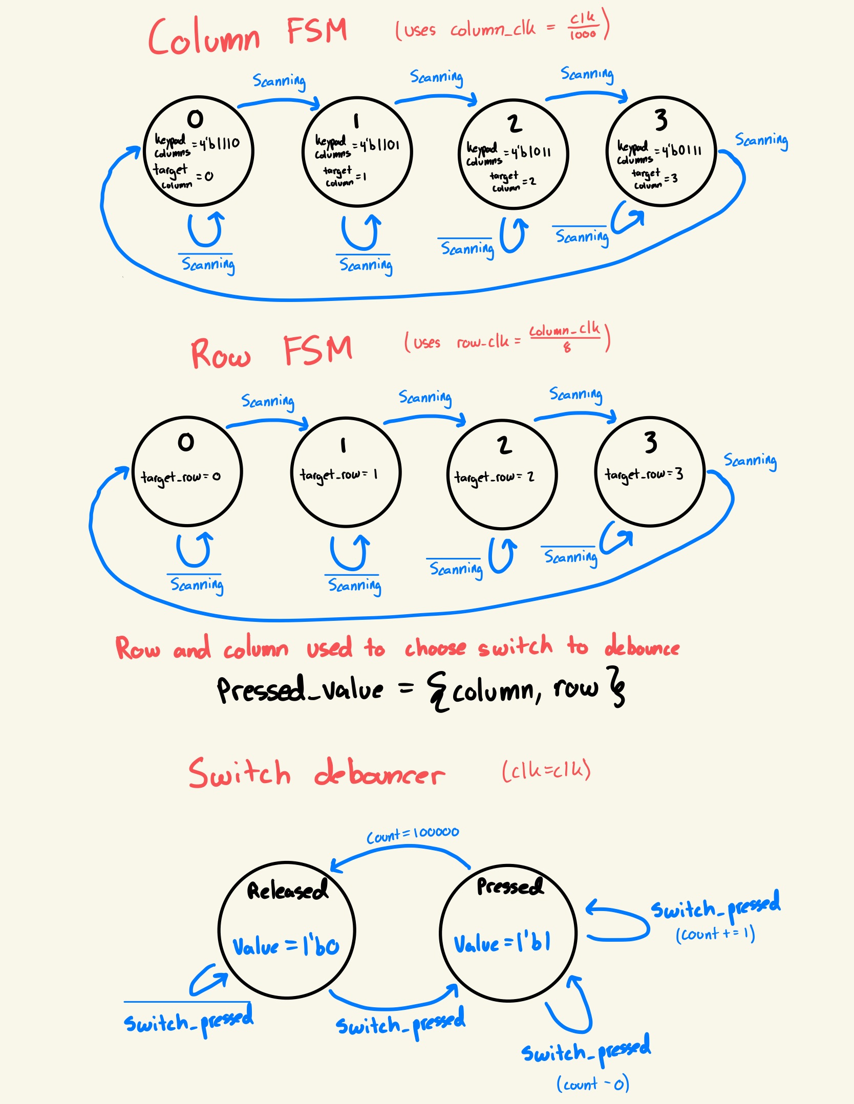
The on-board high-speed oscillator (HSOSC) from the iCE40 UltraPlus primitive library was used to generate a clock signal at 48 MHz. A clock divider is then used to reduce the clock in several key ways. The original clock is reduced by 200000 to create the signal used to display the two previous digits on 2 seven-segment displays with only 9 wires as achieved in the previous lab. The original clock is also reduced by 2000 to scan the rows of the keypad, and the row clock is then reduced by another 16 times to create the column clock which is then used to scan the columns. These clocks drive a series of flip flops with adders connected to themselves to iterate over the columns and rows of the keypad. These counts are used to mux the switches into a single switch debouncer, and when the switch has registered a press, all counters stop until the switch is released. A keypress is registered by first passing through a synchronizer to stablize the input, then through a switch debouncer. The switch debouncer functions by moving to a “Pressed” state upon a high input signal, but will only move to a “Released” state after registering no high input signal for 100000 clock cycles.
This method of switch debouncing was chosen because it provides near immediate on-press stimulus to the circuit, and has no noticeable drawbacks for the keypad used. It is important to consider that this design only works effectively because there is no debouncing required for when the switch is released. If in application, there is often caseonarios where two switches are being pressed at the same time or that the switch has “phantom presses” or needs to be debounced on release, another design method should be chosen.
Some other example switch control mechanisms would be to have a 2 way gated press/release meaning a count has to be hit before a press is registered as well. This comes with the tradeoff of being slower to register a key press, but would function very well in a situation with “phantom presses” or the need for release debouncing. Another method would to have a buffer for each switch and when the buffer is full a key press is registered, this allows the advantage of selecting multiple keys at the same time but would require substantially more hardware to be effective.
Technical Documentation
The source code for the project can be found in the associated Github repository.
Block Diagram
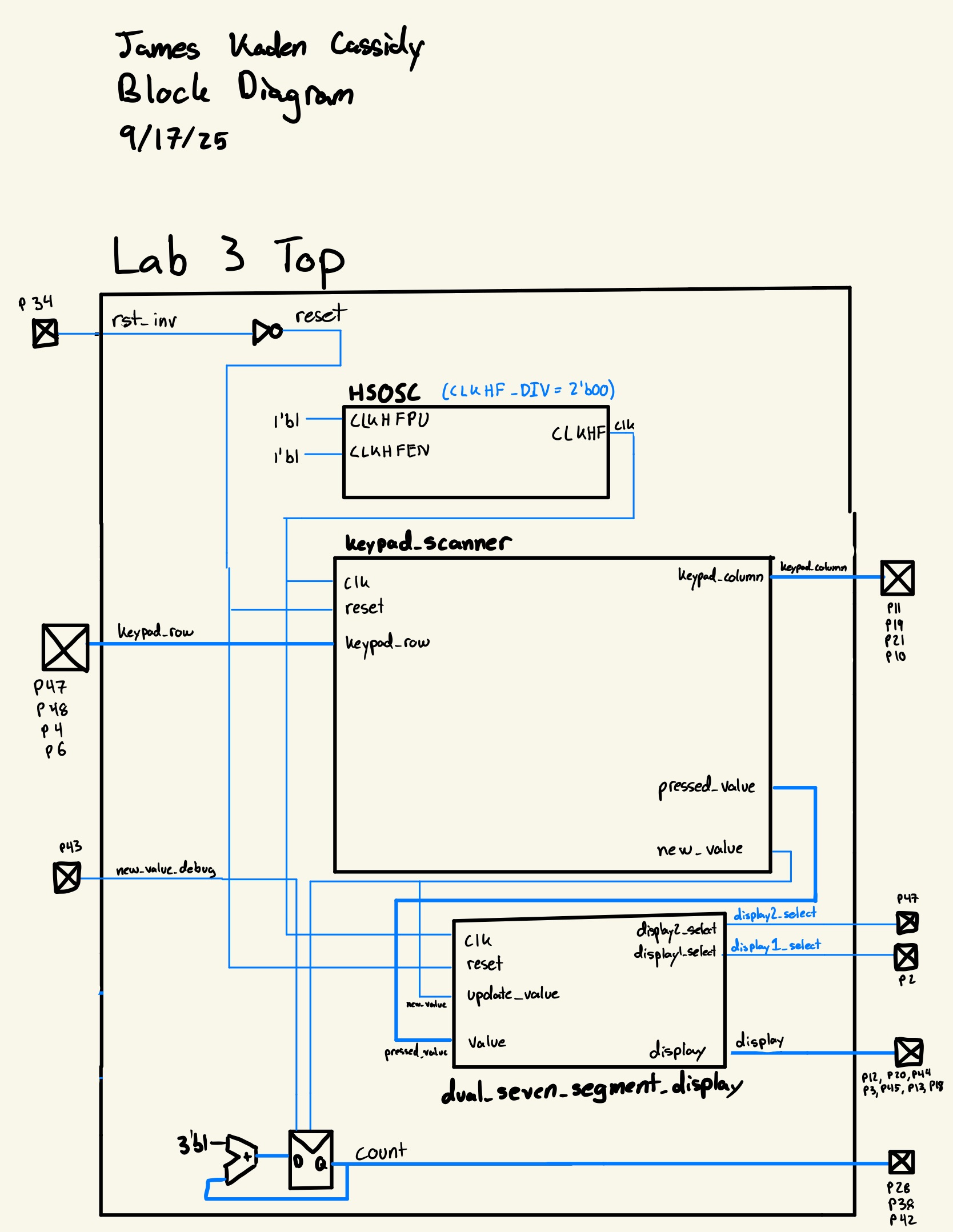
The block diagram gives a high-level schematic of the overall design. The top module include the high-speed oscillator, keypad scanner, and dual seven-segment display driver as well as an adder used to count new key presses.
Schematic
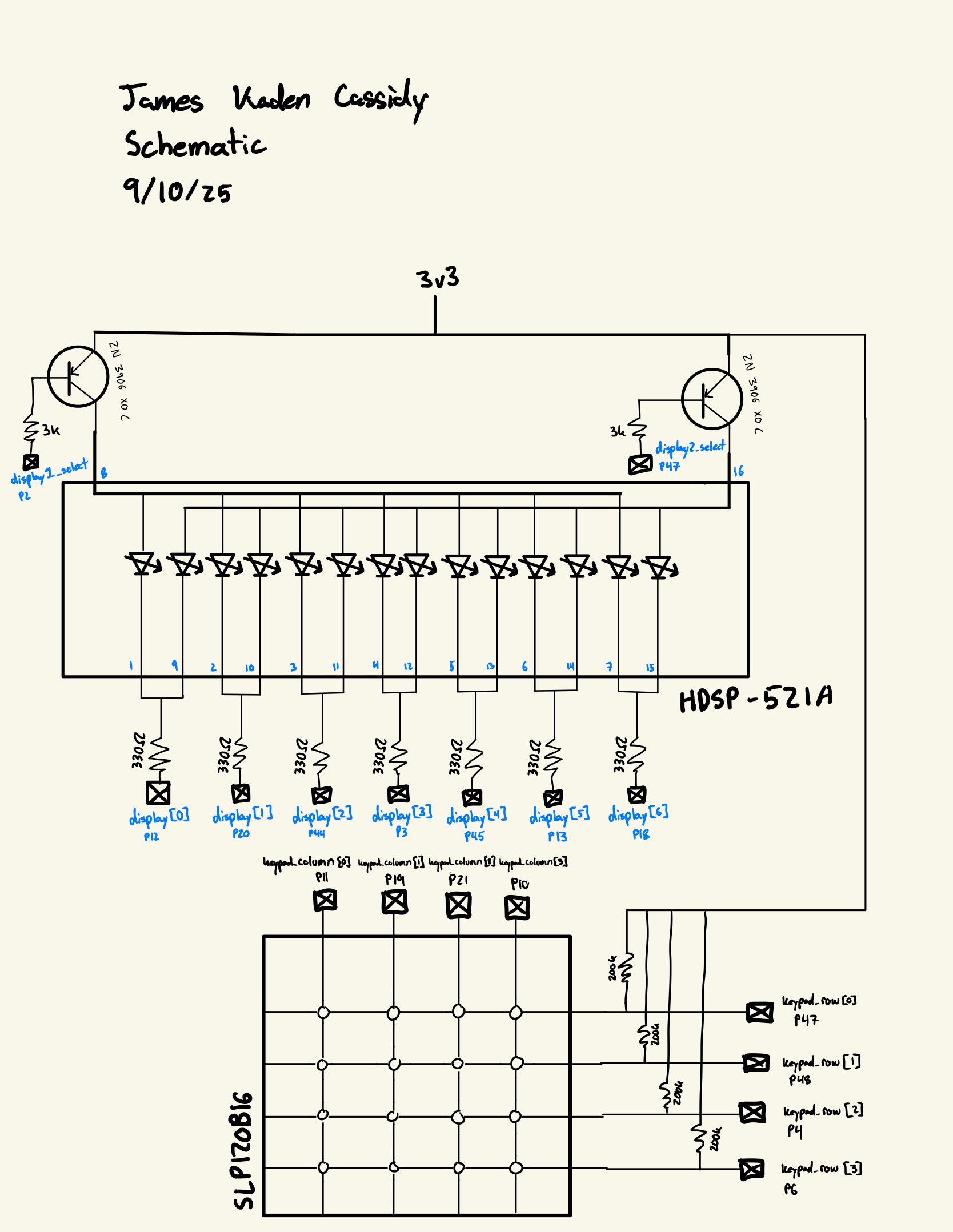
The schematic gives the design of the circuit breadboarded, the general idea is that the two common terminals of the seven-segment displays are connected and then connected through a 330 ohm resistor to an FPGA pin. The power terminal for each display is connected to the collector of a transistor where the base is connected to an FPGA pin through a 3k resistor. The emitter is then connected to the 3v3 line and this setup allows for 9 pins to control 2 seven-segment displays.
The keypad rows are connected as inputs with external 200k pullup resistors for redundancy and the columns are connected directly to FPGA pins to be driven
Results and Discussion
I was able to successfully complete the entire lab with everything functioning correctly. The system is quick and reliable, and I am very satisfied with the product.
Testbench Simulation
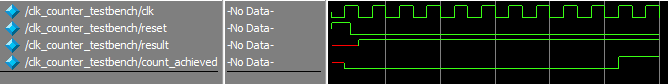
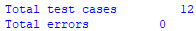
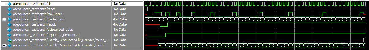
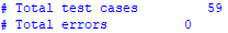

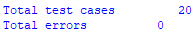

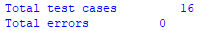
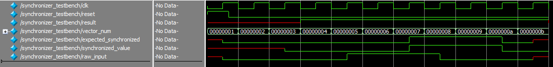
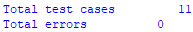
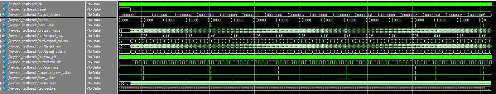
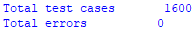
The testbenches were used to confirm that the clk counter correctly triggers, the debouncer properly debounces, the dual segment display correctly displays both values, the synchronizer correctly passes through the values, and that the debugging leds in the top module work as expected.
Conclusion
To complete this lab, I began by wiring the breadboard carefully. I then wrote the Verilog modules and testbenches to test any I had modified or created. I ended up making several simple mistakes while writing the Verilog for this project that were difficult to debug. In the future I will begin by more carefully reviewing the net list diagram before attempting debugging in another manner as the mistakes I made were very obvious in this diagram. This lab took me 10 hours to complete.
AI Prototype Summary
In this lab I analyzed giving Chat GPT 5 two different types of prompts to complete the lab: 1 shot, and multiple steps.
Link to multiple step transcript
Considering the two side by side I think there are advantages to each. The advantage of the 1 shot is allowed the most flexibility of design, for someone who isn’t sure about the best approach to go with, it can optimize at a higher level before getting into the specifics of a design. The disadvantage, and the advantage of the multi-step method, is if one already has a design structure in mind and simply wants the chat bot to create this vision, the 1 shot method doesn’t follow that closely, while the multiple step method allows for a specific design of one module that is then integrated by further modules generated.
For a hardware designer I would recommend the multi-step process as it forces the designer to already have a clear vision of the hardware, which is important to have before writing code. While I could understand the general scheme of what the LLM was trying to do, it was very difficult to envision the hardware which I believe is strongly counterproductive to good hardware design.